- 您现在的位置:买卖IC网 > Sheet目录3882 > PIC18F4539-I/ML (Microchip Technology)IC MCU FLASH 12KX16 EE A/D 44QFN
2002 Microchip Technology Inc.
Preliminary
DS30485A-page 187
PIC18FXX39
18.4
A/D Conversions
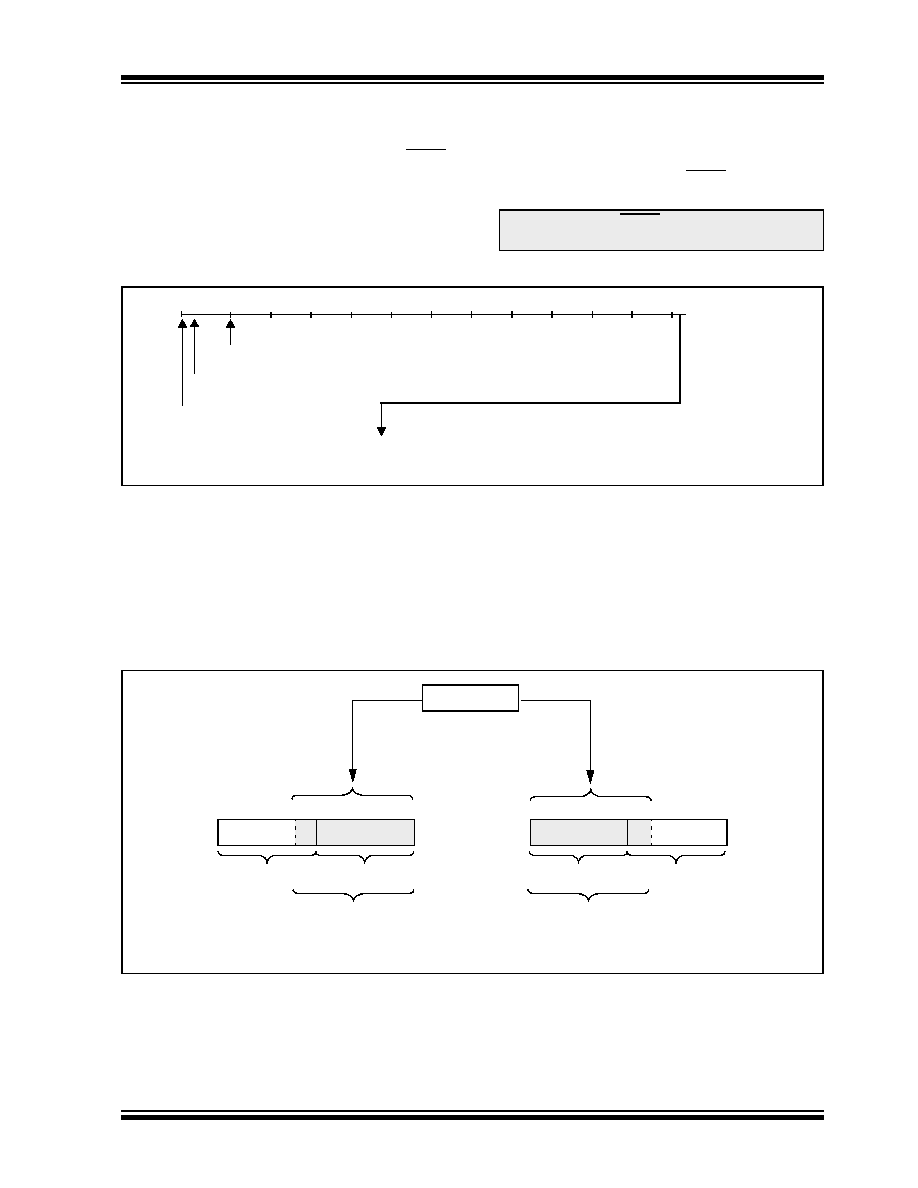
Figure 18-3 shows the operation of the A/D converter
after the GO bit has been set. Clearing the GO/DONE
bit during a conversion will abort the current conver-
sion. The A/D result register pair will NOT be updated
with the partially completed A/D conversion sample.
That is, the ADRESH:ADRESL registers will continue
to contain the value of the last completed conversion
(or the last value written to the ADRESH:ADRESL reg-
isters). After the A/D conversion is aborted, a 2 TAD wait
is required before the next acquisition is started. After
this 2 TAD wait, acquisition on the selected channel is
automatically started. The GO/DONE bit can then be
set to start the conversion.
FIGURE 18-3:
A/D CONVERSION TAD CYCLES
18.4.1
A/D RESULT REGISTERS
The ADRESH:ADRESL register pair is the location
where the 10-bit A/D result is loaded at the completion
of the A/D conversion. This register pair is 16-bits wide.
The A/D module gives the flexibility to left or right justify
the 10-bit result in the 16-bit result register. The A/D
Format Select bit (ADFM) controls this justification.
Figure 18-4 shows the operation of the A/D result justi-
fication. The extra bits are loaded with ‘0’s. When an
A/D result will not overwrite these locations (A/D
disable), these registers may be used as two general
purpose 8-bit registers.
FIGURE 18-4:
A/D RESULT JUSTIFICATION
Note:
The GO/DONE bit should NOT be set in
the same instruction that turns on the A/D.
TAD1 TAD2 TAD3 TAD4 TAD5 TAD6 TAD7 TAD8
TAD11
Set GO bit
Holding capacitor is disconnected from analog input (typically 100 ns)
b9
b8
b7
b6
b5
b4
b3
b2
TAD9 TAD10
b1
b0
TCY - TAD
Next Q4: ADRESH/ADRESL is loaded, GO bit is cleared,
ADIF bit is set, holding capacitor is connected to analog input.
Conversion Starts
b0
10-bit Result
ADRESH
ADRESL
0000 00
ADFM = 0
0
2 1 0 7
7
10-bit Result
ADRESH
ADRESL
10-bit Result
0000 00
7
0 7 6 5
0
ADFM = 1
Right Justified
Left Justified
发布紧急采购,3分钟左右您将得到回复。
相关PDF资料
PIC18F4439-I/ML
IC MCU FLASH 6KX16 EE A/D 44QFN
PIC18F2439-I/SO
IC MCU FLASH 6KX16 EE A/D 28SOIC
PIC16F687-I/SO
IC PIC MCU FLASH 2KX14 20SOIC
PIC16F877AT-I/PTG
IC MCU FLASH 8KX14 W/AD 44 TQFP
PIC16F877A-I/LG
IC MCU FLASH 8KX14 W/AD 44PLCC
PIC12LC509AT-04I/MF
IC MCU OTP 1KX12 LV 8-DFN
PIC12C509AT-04I/MF
IC MCU OTP 1KX12 8-DFN
PIC24F08KL301-I/SS
IC MCU 16BIT 8KB FLASH 20-SSOP
相关代理商/技术参数
PIC18F4539-I/P
功能描述:8位微控制器 -MCU 24KB 1408 RAM 32 I/O RoHS:否 制造商:Silicon Labs 核心:8051 处理器系列:C8051F39x 数据总线宽度:8 bit 最大时钟频率:50 MHz 程序存储器大小:16 KB 数据 RAM 大小:1 KB 片上 ADC:Yes 工作电源电压:1.8 V to 3.6 V 工作温度范围:- 40 C to + 105 C 封装 / 箱体:QFN-20 安装风格:SMD/SMT
PIC18F4539-I/P
制造商:Microchip Technology Inc 功能描述:IC 8BIT FLASH MCU 18F4539 DIP40
PIC18F4539-I/PT
功能描述:8位微控制器 -MCU 24KB 1408 RAM 32 I/O RoHS:否 制造商:Silicon Labs 核心:8051 处理器系列:C8051F39x 数据总线宽度:8 bit 最大时钟频率:50 MHz 程序存储器大小:16 KB 数据 RAM 大小:1 KB 片上 ADC:Yes 工作电源电压:1.8 V to 3.6 V 工作温度范围:- 40 C to + 105 C 封装 / 箱体:QFN-20 安装风格:SMD/SMT
PIC18F4539IPT
制造商:MICRO CHIP 功能描述:NEW
PIC18F4539T-E/ML
功能描述:8位微控制器 -MCU 24KB 1408 RAM 32 I/O RoHS:否 制造商:Silicon Labs 核心:8051 处理器系列:C8051F39x 数据总线宽度:8 bit 最大时钟频率:50 MHz 程序存储器大小:16 KB 数据 RAM 大小:1 KB 片上 ADC:Yes 工作电源电压:1.8 V to 3.6 V 工作温度范围:- 40 C to + 105 C 封装 / 箱体:QFN-20 安装风格:SMD/SMT
PIC18F4539T-E/PT
功能描述:8位微控制器 -MCU 24KB 1408 RAM 32 I/O RoHS:否 制造商:Silicon Labs 核心:8051 处理器系列:C8051F39x 数据总线宽度:8 bit 最大时钟频率:50 MHz 程序存储器大小:16 KB 数据 RAM 大小:1 KB 片上 ADC:Yes 工作电源电压:1.8 V to 3.6 V 工作温度范围:- 40 C to + 105 C 封装 / 箱体:QFN-20 安装风格:SMD/SMT
PIC18F4539T-I/ML
功能描述:8位微控制器 -MCU 24KB 1408 RAM 32 I/O RoHS:否 制造商:Silicon Labs 核心:8051 处理器系列:C8051F39x 数据总线宽度:8 bit 最大时钟频率:50 MHz 程序存储器大小:16 KB 数据 RAM 大小:1 KB 片上 ADC:Yes 工作电源电压:1.8 V to 3.6 V 工作温度范围:- 40 C to + 105 C 封装 / 箱体:QFN-20 安装风格:SMD/SMT
PIC18F4539T-I/PT
功能描述:8位微控制器 -MCU 24KB 1408 RAM 32 I/O RoHS:否 制造商:Silicon Labs 核心:8051 处理器系列:C8051F39x 数据总线宽度:8 bit 最大时钟频率:50 MHz 程序存储器大小:16 KB 数据 RAM 大小:1 KB 片上 ADC:Yes 工作电源电压:1.8 V to 3.6 V 工作温度范围:- 40 C to + 105 C 封装 / 箱体:QFN-20 安装风格:SMD/SMT